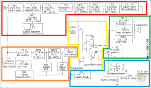
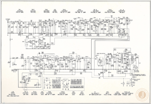
I will briefly explain the function of each circuit block, which is always based on a semiconductor component. The surrounding components are there to support / complete that specific semiconductor in various ways.
3.2.1 FM Circuit:
TR1 = Transistor 1: FM aerial radio frequency (RF) preamplifier, of the whole UKW (Ultra-short-wave) band
TR7 = Transistor 7: FM Frequency oscillator (sets the filter-frequency for the tuned FM radio station)
TR2 = Transistor 2: FM Mixer converter: Converts the aerial frequency down to the intermediate frequency
D3 = Diode 3: FM AFC. Auto frequency control: Ensures the tune remains on the set radio frequency
TR3 = Transistor 3: First FM intermediate frequency preamplifier
TR4 = Transistor 4: Second FM intermediate frequency preamplifier
TR5 = Transistor 5: Third FM intermediate frequency preamplifier
TR6 = Transistor 6: Fourth FM intermediate frequency preamplifier
D1 / D2 = Diode 1 & 2: FM Ratio detector demodulator (demodulates the frequency modulated (FM) radio signal into an actual audio signal)
The ratio detector is a relatively basic FM Demodulator design, but one that works very well without using too many components
3.2.2 AM Circuit:
TR 11 = Transistor 11: AM Frequency oscillator (filter-sets the frequency for the tuned AM radio station)
D8 = Diode 8: Oscillation / feedback prevention: Ensures that the whole circuit does not start to resonate / oscillate
TR8 = Transistor 8: AM Mixer converter: Converts the aerial frequency down to the intermediate frequency
TR9 = Transistor 9: First AM intermediate frequency preamplifier
D5 = Diode 5 = AGC / AVR = Automatic Gain Control (for stable output signal)
TR10 = Transistor 10: Second AM intermediate frequency preamplifier
D6 = Diode 6 = AGC / AVR = Automatic Gain Control (for stable output signal)
D7 = Diode 7 = AM Demodulator (demodulates the Amplitude modulated (AM) radio signal into an actual audio signal
3.2.3 Amplifier circuit
IC = Integrated circuit FA6007T: Audio preamplifier and Power amplifier driver xircuit.
ZD1 = Z-diode 1: Voltage stabilization of the Amplifier circuitry.
D9 = Diode 9: Temperature compensation of the amplifier circuitry.
TR12 & TR13: Transistor 12 / 13: Power output amplifier stage.
3.2.4 Circuit design details:
If you want to google more:
TR1 is an NPN-transistor used in “basic-circuit” design
TR2-11 are all NPN-transistors, used in the so-called “emitter-circuit” design
TR12 & 13 are used in a so-called Push-and-Pull power amplifier circuit design, where one transistor works for the positive half of the sinewave-signal, and the second transistor amplifies the negative half of the signal.
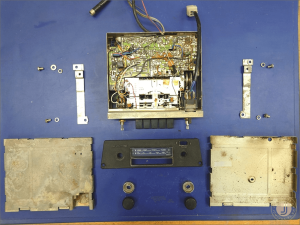
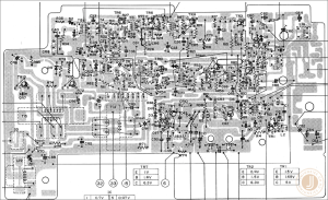
3.3 PCB Layout
Looking at such a PCB (Printed circuit board) layout these days (where computer aided PCB layout with automated trace routing is the norm), drives my OCD nuts, but at the same time such a hand-drawn layout was standard at that time.
The gray areas show the copper traces on the PCB, and the black items are the various electronic components (standardized symbols). The numbers next to it refer to the numbers in the detailed wiring / block diagrams.
The trace design of high frequency circuits and audio PCB’s have come a long way since then, so it’s not really an optimal design when it comes to noise protection, etc. But from my experience it still works pretty well.
 Nils Ehrat